SuperRT
December 13, 2020
Video links for this article:
Update 31th May 2021: The source code for SuperRT has now been released.
I’m pleased to finally have some results to show for a project I’ve been working on in my spare time for the last year or so.
The idea originated when I was trying to think of an interesting idea for a project to help me learn Verilog and FPGA design, and the notion of building a simple raytracer came to mind (partly inspired by a scarily smart friend of mine who is building his own GPU). A bit later - because sometimes my brain hates me and delights in coming up with silly things to do - this turned into “wouldn’t it be interesting to try making a SNES do raytracing?”, and thus the SuperRT chip idea was born.
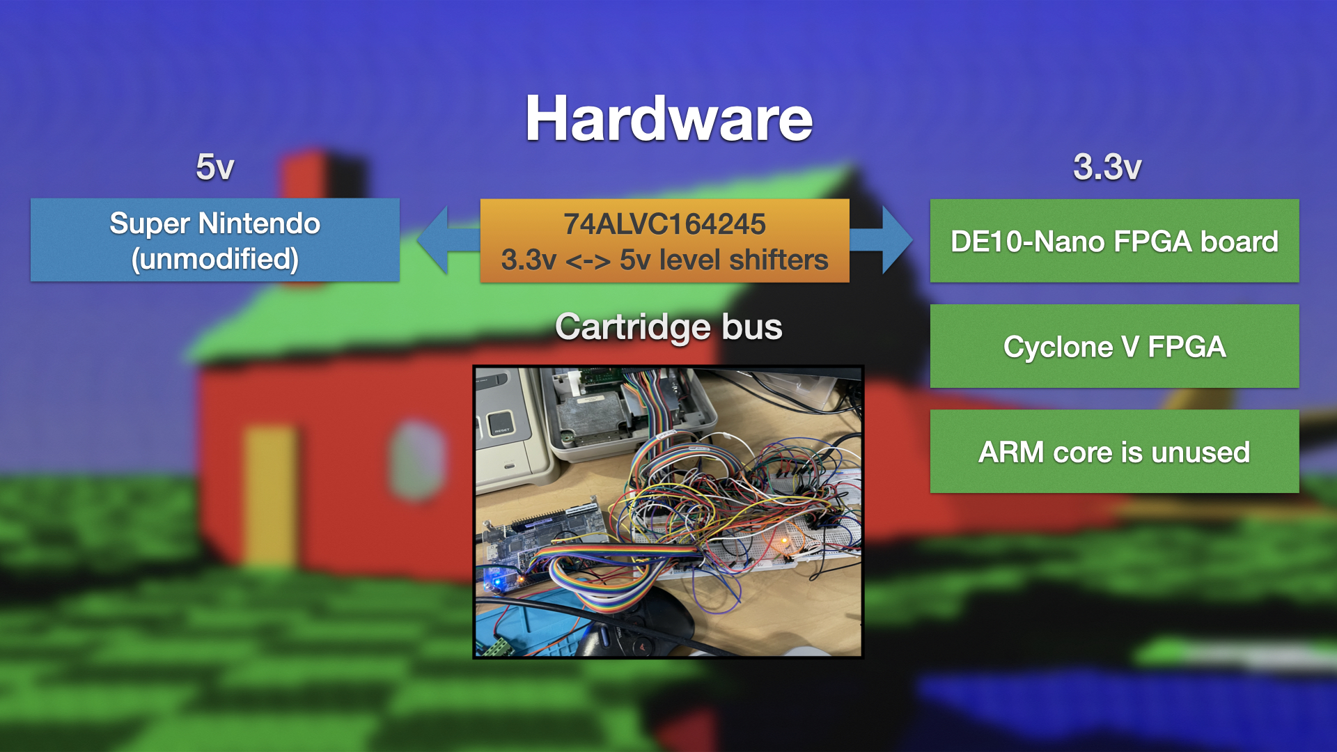
What I wanted to try and do was something akin to the Super FX chip used in titles such as Star Fox, where the SNES runs the game logic and hands off a scene description to a chip in the cartridge to generate the visuals. To that end I’ve deliberately tried to restrict myself to just using a single custom chip for the design, not making use of the ARM core available on the DE10 board or any other external processing resources.
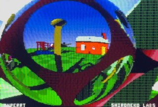
The end results look something like this:
Apologies for the poor screenshot quality, incidentally - for some reason my capture card produces terrible results when capturing from my SNES, so I had to resort to the good old “photograph the screen in a darkened room” approach.
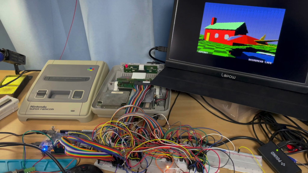
The Super Nintendo (technically a Super Famicom) seen here has had the case removed to make room for the cabling, but other than that is totally unmodified. Attached to it is the PCB from a copy of an awful Pachinko game I picked up for 100 yen at a local second-hand store, with the game ROM removed and replaced with a cable breakout. This then passes through a set of level shifters to convert the SNES’s 5v down to 3.3v and then into a DE10-Nano FPGA development board with a Cyclone V FPGA. The level shifter boards are anything but pretty - and assembling them was a nightmare thanks to the necessary ICs only being available in surface-mount packages - but they do the job.
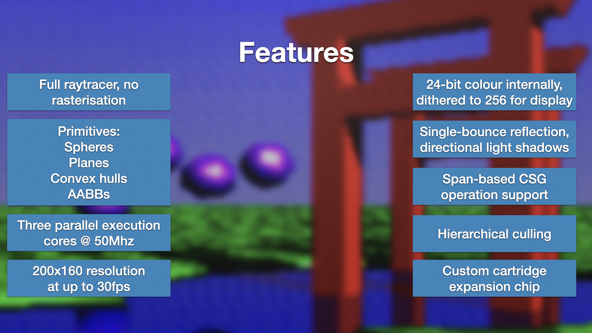
The SuperRT chip constructs the scene using a specialised command language which is executed by one of three parallel execution units on the chip - essentially specialised CISC processors - to perform ray intersection tests. The scene description allows objects to be constructed using a subset of CSG operations, using spheres and planes as the basic building blocks and then performing OR, AND and subtraction operations using them to build up the desired geometry. AABBs are also supported, although primarily for use in culling tests (they can be rendered if desired, but they have a lower positional accuracy than other primitives and thus this is not generally very useful except for debugging purposes).
The renderer casts up to four rays per screen pixel, calculating direct shadows from a directional light source and a single reflection bounce. Surfaces each have a diffuse colour and reflectivity property, and it’s possible to apply modifiers to these based on CSG results or specialised functions - this is used to generate the checkerboard pattern on the floor.
The ray colour for each pixel is calculated by a “ray engine”, which handles the overall ray lifecycle and uses an “execution engine” module to run the command program describing the scene as many times as is required to resolve the ray. The command program itself is uploaded from the SNES and stored in a local 4K RAM buffer - animation is performed by writing modified commands into this buffer as required. A disassembled command buffer looks like this:
0000 Start
0001 Plane 0, -1, 0, Dist=-2
0002 SphereSub OH 2, 1, 5, Rad=5
0003 SphereSub OH 4, 1, 4, Rad=4
0004 SphereSub OH 5, 1, 9, Rad=9
0005 SphereSub OH 2, 1, 2, Rad=2
0006 SphereSub OH -0.5, 1, 2, Rad=2
0007 RegisterHitNoReset 0, 248, 0, Reflectiveness=0
0008 Checkerboard ORH 48, 152, 48, Reflectiveness=0
0009 ResetHitState
0010 Plane 0, -1, 0, Dist=-2.150146
0011 RegisterHit 0, 0, 248, Reflectiveness=153
0012 AABB 4, -2.5, 11,    8, 3.5, 13
0013 ResetHitStateAndJump NH 44
0014 Origin 6, 2, 12
0015 Plane -0.2929688, 0, -0.9570313, Dist=0.2497559
0016 PlaneAnd OH 0.2919922, 0, 0.9560547, Dist=0.25
0017 PlaneAnd OH 0, 1, 0, Dist=1
0018 PlaneAnd OH 0, -1, 0, Dist=4
0019 PlaneAnd OH -0.9570313, 0, 0.2919922, Dist=-1
0020 PlaneAnd OH 0.9560547, 0, -0.2929688, Dist=1.499756
0021 RegisterHit 248, 0, 0, Reflectiveness=0
Each execution engine is a processor module with a 14 cycle pipeline, and in general one instruction is retired per cycle, so each execution unit can calculate about 50 million sphere, plane or AABB intersections per second. The exception to this is that branch operations have to flush the entire pipeline and thus have a 16 cycle overhead (14 cycles to flush the pipeline + 2 cycles instruction fetch delay). To try and avoid this as much as possible a branch prediction system is used - fortunately a lot of the time the spatial coherency of nearby rays means that a high prediction hit rate is achievable.
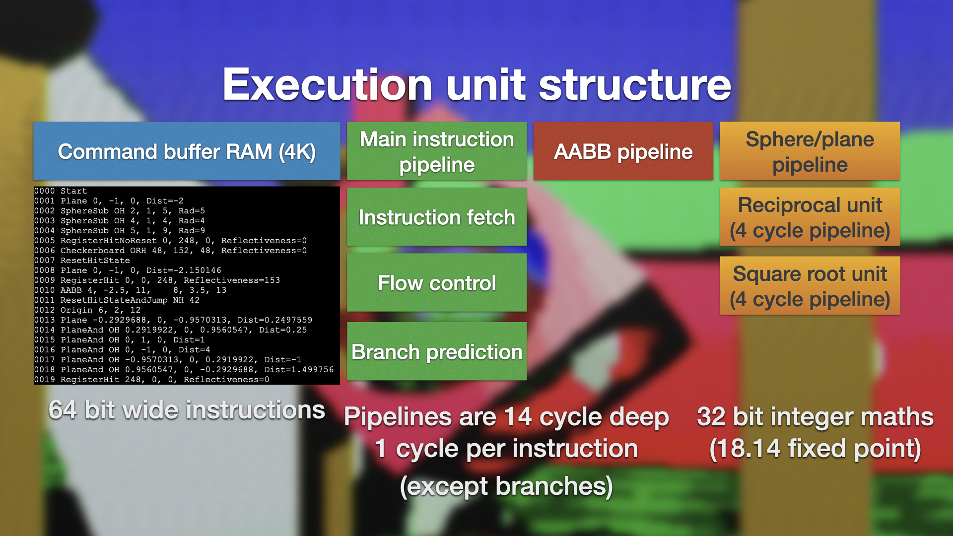
Intersections in the execution engine are carried out by two pipelines, one handling AABBs and the other spheres and planes. The system as a whole works exclusively using 32-bit integer maths in 18.14 fixed point format, with 16-bit (2.14) format used where values are known to be in the +-1 range, and the sphere/plane intersection pipeline has two dedicated additional maths units that calculate reciprocal and square root operations.
Once a frame is rendered, the PPU converter module turns the framebuffer into a format that can be DMAed directly to the SNES VRAM for display, reducing it to 256 colours and swizzling it into character tile bitplanes. The screen resolution is 200x160 - this results in exactly 32000 bytes of image data for a full frame, which is transferred to VRAM in two 16000 bytes chunks over successive frames due to bandwidth constraints. Thus the full image can only be refreshed once every two frames, effectively limiting the maximum framerate to 30FPS - although the test scene runs at closer to 20FPS (primarily due to some bottlenecks with the logic on the SNES side at present).
Many thanks to the participants in this thread over at SNESdev for a lot of useful ideas on fullscreen expansion chip DMA that inspired the solution used here.
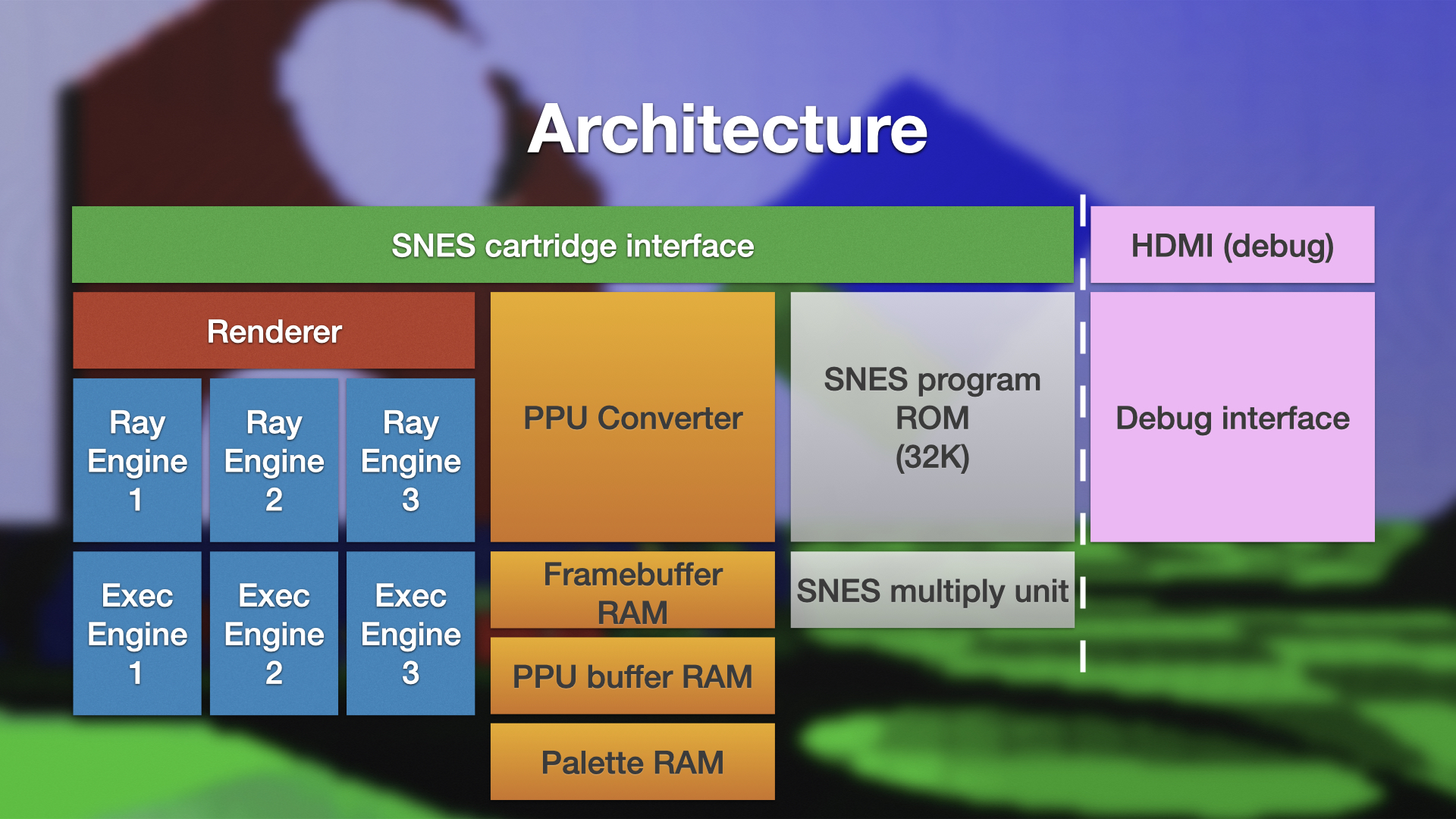
The chip also implements a number of other basic functions - there is an interface to the SNES cartridge bus, along with a small program ROM holding 32K of code for the SNES (this is constrained by the fact that the interface board currently only connects up the SNES Address Bus A lines, and thus the effective usable address space is a mere 64K, of which 32K is used for memory-mapped IO registers to communicate with the SuperRT chip). There is also a multiplication accelerator unit that lets the SNES perform 16x16bit multiply operations rapidly.
For debugging, I used the HDMI interface on the DE10 board to output data to a second monitor, along with a Megadrive joypad connected to the GPIO pins to manipulate the debug system. Resource constraints mean that this has to be disabled if all three ray engine cores are enabled, however.
So that’s a broad overview of the system - I intend to post some articles giving more details of how individual components work in the near future. In the meantime, though, if you have any questions or thoughts then please get in touch and I’ll do my best to answer!
Many thanks to Matt, Jaymin, Rick and everyone else who has helped with advice, inspiration and support!
“SNES” and “Super Nintendo” are trademarks of Nintendo Co Ltd. This is a hobby project and completely unassociated with Nintendo.